Analog and digital microelectronics
Our circuits are located right at the interface between the real analog world and the data processing functions. Conscious that most of the modern electronic applications merge analog functions and digital intelligence, ID MOS accumulated more than 15 years of experience in the domain of mixed-signal micro-electronics. Our ASIC design teams are very much specialized: depending on your needs, analog and digital engineers are organized in a project team to develop jointly your dedicated integrated circuit.
With the experience of about 200 ASIC design projects, ID MOS capitalized a large IP library and reusable standard analog blocks allowing cost and planning optimization.


Methodology and expertise
We are experts in ASIC design. Our development methodologies meet world standards. Our approach is particularly strict towards the implementation of your requirements inside the ASIC, as well as the associated verification processes. All our designs include a comprehensive testability study which prefers in situ techniques to optimize the electrical test conditions and target zero defect on mass production.
Beyond our standard methodologies, we offer to develop according to specific workflows, applying design guidelines and requirements driven by DO254 standard or other equivalent.

For more than 15 years, we have been addressing multiple demanding segments, which cross-fertilized our working methodologies. We gather a strong multi-domain expertise. Industrial segments such as transportation and harsh environments became one of our poles of excellence, with circuits dedicated to sensor signal acquisition, instrumentation and Systems-on-Chip.
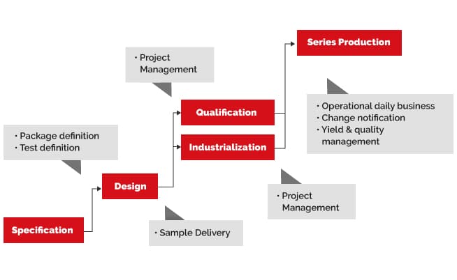
Each ASIC is developed with the perspective of its later series production. ID MOS takes care of the whole industrialization and the manufacturing. We use long term partnerships with state-of-the art world-class suppliers chosen on such criteria as technologies long life time, quality and process control and cost effectiveness.
Our design may target a wide technology spectrum with nodes ranging from 1µm down to 65nm, including analog oriented process features and high-voltage capability. That allows the best process fit for a given IC, and also the most appropriate performance/cost trade-off.
Our ASICs are packaged by the IC assembly leaders, offering the availability of a large package collection starting from the old-fashioned DIP up to the most recent CSP packages, both in ceramic and plastic types.
RADHARD technologies
High-altitude or Space applications require radiation immunity to provide airborne components with reliability and operational life time. Building on the complete development of a 100krad library based on a 350nm technology, ID MOS offers a validated solution bringing the adapted robustness to ASICs specifically designed for these environments.
Beyond TID, our design methodologies ensure a good SEE immunity, both by the quality of our Layouts (SEL), and by the specificity of our architectures (SET, SEFI and SEU).


Extreme temperatures
If the IC working environment temperature exceeds the regular ranges, we may propose ways to extend these temperatures, using foundry processes characterized for that specific purpose. Using our capability to generate models and libraries, ID MOS already characterized a selection of CMOS foundry processes and generated or adapted the corresponding Process Design Kits allowing circuit functions at very cold temperature (down to -193K), and very hot temperatures (up to 225°C for regular CMOS and 300°C for SOI-CMOS).
Secured ASIC
In cooperation with SERMA Safety & Security, ID MOS offers appropriate solutions to secure your ASICs by implementing encrypting and decrypting or by integrating power supply monitoring against external intrusion. Even more advanced features allow dissuasion against copying such as ghost tracks on layout or multiple metal sheilding on the chip.

